
No.33
Hi-Fi Audio
EL509/6KG6
![]()
Direct-Coupled SE Amplifier Using the EL509/6KG6
By: Bob Danielak

 The Svetlana EL509/6KG6 is a
rugged beam tetrode with a plate dissipation rating of 35W.
It may be classified as a "sweep tube" because it
was originally designed as a horizontal sweep amplifier for
TV applications. Its high sensitivity and efficiency allows
for up to 15W output from a single tube. As with any other
beam tetrode or pentode, however, distortion in single-ended
operation can be high. Large amounts of feedback are generally
required to reduce distortion to acceptable levels for audio
reproduction. An interesting mode of operating sweep tubes
is known as "screen drive", or sometimes "enhanced
triode mode". In this arrangement the audio signal is
applied to the screen grid (g2 or "screen", for
short) instead of the Control Grid (g1 or "grid"
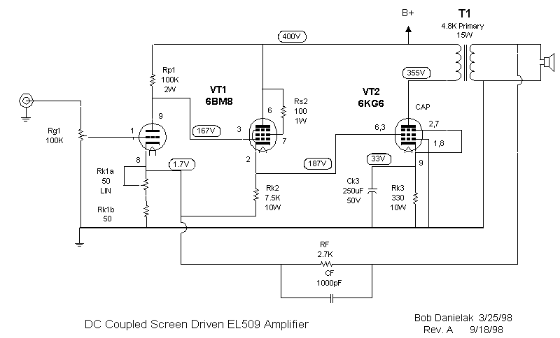
for short). This arrangement can be seen in the circuit schematic
in Figure 1. Screen drive is generally much more linear than
standard tetrode or pentode operation; such that lower levels
of feedback are required. Therefore, this type of circuit
lends itself more easily to Hi-Fi applications.
The Svetlana EL509/6KG6 is a
rugged beam tetrode with a plate dissipation rating of 35W.
It may be classified as a "sweep tube" because it
was originally designed as a horizontal sweep amplifier for
TV applications. Its high sensitivity and efficiency allows
for up to 15W output from a single tube. As with any other
beam tetrode or pentode, however, distortion in single-ended
operation can be high. Large amounts of feedback are generally
required to reduce distortion to acceptable levels for audio
reproduction. An interesting mode of operating sweep tubes
is known as "screen drive", or sometimes "enhanced
triode mode". In this arrangement the audio signal is
applied to the screen grid (g2 or "screen", for
short) instead of the Control Grid (g1 or "grid"
for short). This arrangement can be seen in the circuit schematic
in Figure 1. Screen drive is generally much more linear than
standard tetrode or pentode operation; such that lower levels
of feedback are required. Therefore, this type of circuit
lends itself more easily to Hi-Fi applications.
This application note will document a typical screen driven amp design. It is based upon various constraints, trade-offs, limitations and goals, which may be modified by the (experienced) end user to fit his own needs or tastes. The final amplifier produces about 10W with reasonably low distortion while using a minimal amount of negative feedback. (Please note that constructing this amplifier requires some technical skill; therefore, it is not recommended as a DIY project for the novice.)
Background:
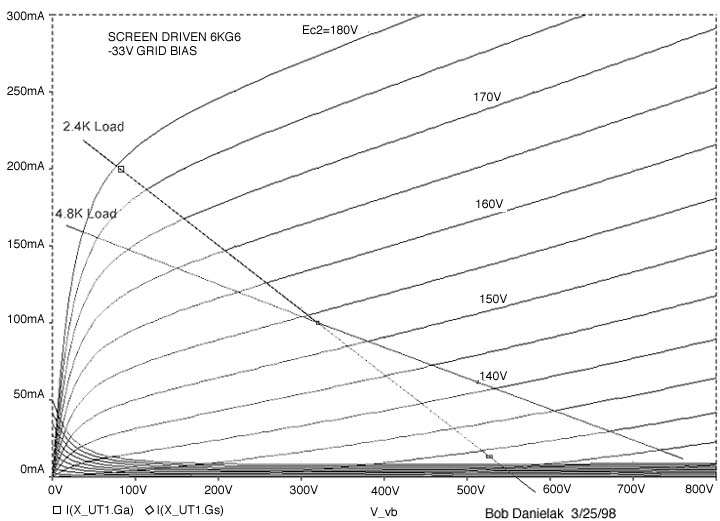
Although screen drive has been employed by many designers over the years, there is currently very little published reference material on the subject. Screen bias curves (plate curves for a fixed grid bias and various screen voltages) are generally not published. And if they are, it is usually only for a zero grid bias. Although the required information can be interpolated using a tube characteristic "nomograph", the process would be quite tedious.
Luckily, we are able to take advantage of modern computer simulation tools to do this work for us. This design effort relied heavily upon a PSPICE model of the 6KG6/EL509 provided by Duncan Munro on his web site (listed elsewhere on the Svetlana home page). This model was used to develop a full set of screen bias curves for the desired grid bias. Actual test data was closely correlated with the model.
Design/Discussion:
Screen bias curves are given in the Svetlana EL509 data sheets. These curves are given for zero grid bias. The phenomenal input sensitivity displayed by these curves, however, is really a double-edged sword. Because the screen draws varying (signal-dependent) current from the driver, it is best to DC couple the driver. Keeping the DC bias stable with such a high screen sensitivity would be a challenge, especially using all tube circuitry. One solution is to provide some negative grid bias to reduce the screen sensitivity. This has the added benefit of increasing the required DC screen potential for a given quiescent plate current. This makes DC coupling that much easier, since the preceding stage plate voltages are generally 100V or more.
The simplest way of providing the required grid bias is by using cathode bias. This arrangement is self-compensating, so it will further enhance DC stability. For this design, a grid bias of -33V was chosen. (This was actually an iterative process based upon the desired plate current and screen voltage levels.) The screen bias curves for -33V bias are given in Fig. 2. Note that Fig. 2 also includes screen current curves. Screen current is surprisingly low (<10mA). The operating point was chosen based upon two component limitations. Maximum plate dissipation for the EL509 is 35W, and the maximum DC current allowed in the output transformer is 110mA. So a plate voltage of about 35W / 110mA = 318V could be used. But for conservatism, the combined plate and screen current was reduced to 100mA. This determines that the cathode resistor is to be 330 ohms. Since it will dissipate 33V **2 /330 = 3.3W a wire-wound resistor rated for 10 W, or more, is recommended.
Referring to the characteristics of Fig. 2, the required screen voltage at Eb=320V and Ib=100mA is about 154V. Since this voltage is specified with respect to the cathode, the actual screen potential (measured with respect to ground) would be 154V plus the 33V of cathode bias, or 187V.
The input/driver stage is based upon the Svetlana 6BM8 triode-pentode. The triode section is used as a low distortion gain stage. The power pentode section is used as a high-current, low impedance cathode follower to drive the screen of the EL509 output stage. All three stages are DC coupled. The EL509 screen potential of 187V allows for at least 160V on the plate of the input tube (after considering the bias of the cathode follower stage). This provides for sufficient plate voltage swing and enough bias to provide adequate input signal headroom.
The pentode section is triode-connected by connecting its screen to its plate (via a 100 ohm resistor). This cathode follower stage must be able to supply both the DC and peak screen currents. Therefore the quiescent cathode current is set to about 25mA. Neglecting screen current, the cathode resistor was selected to be 187V / 25mA = 7.5K. This resistor will dissipate 187V **2 / 7.5K = 4.7W, so a 10W, or larger, resistor is required.
The input stage is a little unusual, with a positive feedback connection between the cathode follower stage and the input stage cathode. In a conventional gain stage the cathode resistor is usually bypassed with a large value capacitor to provide an AC short from the cathode to ground. If this capacitor is deleted, the stage gain is reduced due to the negative feedback caused by the ac signal developed across the cathode resistor. In the circuit of Fig. 1 this effect is counteracted by a form of positive feedback from the second stage to the first. The end result is a circuit with almost the same gain as the conventional approach, but without a large (perhaps signal degrading) bypass capacitor. In fact, this approach also saves another resistor, which would have to be inserted in series with the cathode resistor and bypass cap in order to provide a node for the application of loop feedback from the transformer secondary.
Bias adjustment for the amplifier is greatly simplified, though unconventional compared to other SE power-tetrode designs. The output tube bias is controlled by adjusting the operating point of the first gain stage. Balancing all of the voltages throughout the system may seem tricky, but it really is not too complicated once the operating points are worked out. In a conventional gain stage the cathode resistor determines the dc bias based upon its quiescent plate current. In the circuit in Figure 1, the cathode bias is determined by the sum of the plate current and the cathode current of the following stage. Treating the two sections individually, we know the desired cathode bias and operating point for the first stage and the desired cathode current for the second stage, so we can reduce the conventional cathode resistor by a factor of : Ib1 /(Ib1 + Ik2) , where Ib1 is the plate current for the first stage and Ik2 is the cathode current of the second stage. For convenience of balancing the operating points throughout the system, it is suggested that this cathode resistor of the 6BM8 input stage be made adjustable by at least +/- 25%. The cathode resistors of the cathode follower and EL509 output tube do not require adjustment.
Power Supply:
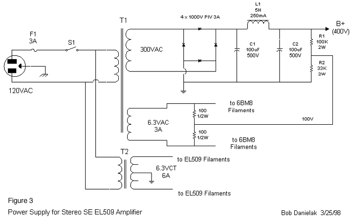
A power supply voltage of about 400V is required to achieve the operating points discussed above. This design assumes about 450 ohms of DC resistance in the output transformer primary. If an output transformer with lower DC resistance value is used, the supply can be lowered accordingly, or the screen voltage may be reduced slightly to lower the plate current. In any case, the maximum plate dissipation of 35W should not be exceeded. It was decided to use the same supply voltage for both the input and output stages. If desired, a decoupling filter may be inserted between the output stage supply and input stage supply. If this is done, a low loss approach (LC filter) is recommended so that maximum signal headroom will be maintained. Perhaps the best place for additional filtering would be between the cathode follower supply and more sensitive input stage supply. In this case, a larger series resistance could be tolerated.
The power supply used for the prototype is shown in Fig. 3. It was based upon a surplus 300VAC power transformer, silicon rectifiers, and capacitor input filter followed by an LC ripple filter. A separate 6.3VAC / 6A filament transformer was used for the EL509 filaments due to uncertainty of the rating of the filament winding on T1. The 6.3VAC supply for the 6BM8 filaments needs to be biased up to 95V (+/- 7V) in order to maintain the 6BM8's heater-cathode potential within +/-100V for both triode and pentode sections. This is done via the voltage divider (R1 and R2) shown in Fig. 3. It would also be acceptable to use a common 6.3VAC winding for both 6BM8's and EL509's provided it was rated for 7A or more. A Hammond 272JX power transformer (600VCT @ 250mA, 6.3VCT @ 8A, 5VCT @4A) appears to be well suited for this application, and would run a stereo pair of amplifiers. Alternate circuits or parts (tube rectifiers, choke input, etc.) may be used if desired. A DC voltage of 375V to 425V is acceptable. However, the screen voltage must be adjusted such that the maximum plate dissipation rating of the EL509 is not exceeded.
Operation/Performance:
Based upon a plate voltage of 320V and a plate current of 100mA, the calculated maximum power output is about 10.6W for a 4.8K plate load, or 10.3W into a 2.4K plate load. These values assume a +/-25V screen signal. Examining these two load lines in Fig. 2, the 2.4K load will result in lower 3rd harmonic distortion at full power while the 4.8K load will result in lower 2nd (and probably lower 3rd) harmonics at lower levels.
Measured power output was between 9-10W at clipping for either plate load. Near full power waveforms looked considerably better using the 2.4K load. However, in listening tests the 4.8K seemed to have a better sound. Keep in mind that average power levels during the listening test were closer to 1 - 2W per channel through speakers having an efficiency of 90dB/W/m. The 2.4K load was achieved by using 8 ohm speakers on the 16 ohm tap of a 4.8K (nominal) output transformer. Any SE output transformer intended for a single 300B is suitable for use in this circuit, as is a transformer with a primary impedance of 4.5k to 5.5k, such as the Hammond 1628SE, One Electron UBT-2, or Electra-Print MT5KB.
Conclusion:
Several interesting features have been employed which improve performance while reducing parts count (cost). Elimination of two coupling caps (via DC coupling throughout) and one bypass cap (via novel cathode positive feedback) improves LF response and the stability of the amplifier by eliminating 4 LF break-points. This unique design also reduces the chance of tonal coloration due to coupling and bypass capacitors.
**The information provided in this application note is intended for general design guidance only. The user assumes all responsibility for correct and safe usage of this information. Svetlana Electron Devices does not guarantee the usefulness or marketability of products based on this material.